
Semiconductor physics is a field of study that provides the core theoretical foundation of modern electronics, and an important discipline that explains how the many electronic devices we use every day work. A semiconductor is a special material with properties intermediate between those of a conductor and an insulator, and it carries electric current through the movement of electrons and holes. Such semiconductor materials serve as the basic materials for devices such as transistors, diodes, and integrated circuits, and on this basis modern electronics has developed rapidly.
This article begins with the physical properties of semiconductors and examines, step by step, how electronic devices operate. It explains the basic theory of semiconductor physics, the conduction band, the band gap, and the process by which current flows through the interaction of electrons and holes, and on that basis covers in detail how various semiconductor devices are designed and operate.
Fundamentals of Semiconductor Physics: The Roles of Electrons and Holes
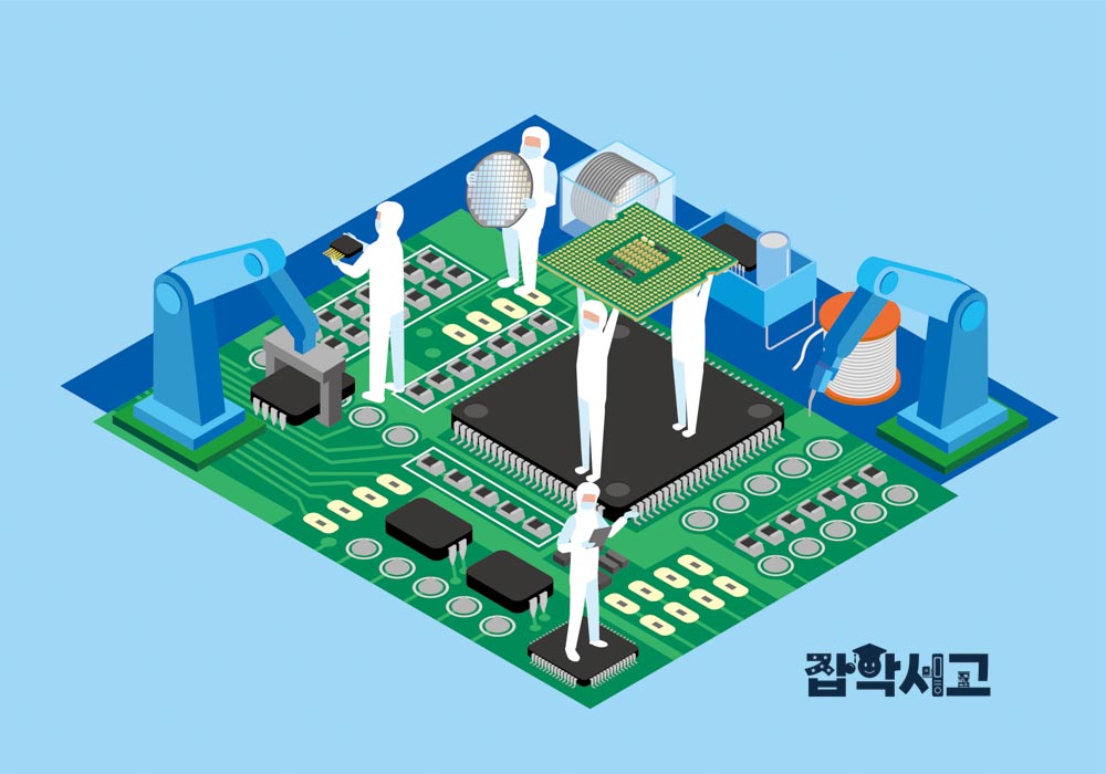
Basic Concepts of Semiconductor Physics
Semiconductor physics is a core principle of modern electronic engineering, a discipline that explains how current flows through the movement of electrons and holes inside a semiconductor. Semiconductors are made of materials such as silicon and gallium arsenide, and these materials conduct current only under certain conditions. These characteristics of semiconductors are determined by how electrons and holes move.
The Roles of Electrons and Holes
In a semiconductor, the electron is a negatively charged elementary particle that can move freely within the crystal structure. Depending on energy levels, electrons can move only when they have a certain energy, and this movement of electrons is what constitutes the flow of current. A hole, on the other hand, is a quasiparticle that treats the vacancy left behind by a departing electron as if it were a positively charged particle. As neighboring electrons fill this vacancy one after another, the hole appears to move in the direction opposite to the electrons, that is, in the direction of the electric field. This movement of electrons and holes is an important factor that determines the electrical properties of a semiconductor.
Conduction Band, Valence Band, and the Band Gap
Within a semiconductor material, electrons can carry current only when they reach a state in which they can move freely. This state is called the conduction band, and here electrons move freely. In contrast, the state of electrons before they move is the valence band, where electrons have relatively low energy. Between the conduction band and the valence band lies an energy interval called the band gap, and for an electron to move into the conduction band, it must overcome this energy gap.
The size of the band gap is one of the important properties of a semiconductor: the narrower this gap, the more easily electrons can move into the conduction band, which increases the semiconductor’s conductivity. When the band gap is wide, conductivity decreases and the semiconductor behaves much like an insulator. The size of the band gap and the movement of electrons and holes have an important influence on the operating principles of semiconductor devices.
Doping and N-type and P-type Semiconductors
In their pure state, semiconductor materials do not conduct current well. However, adding impurities through a process called doping can make current flow more easily. Doping is the artificial control of the number of electrons or holes by adding electrons to or increasing holes in a semiconductor material.
Depending on the doping, semiconductors are divided into N-type and P-type semiconductors. In N-type semiconductors, electrons are the majority carriers, while in P-type semiconductors, holes act as the majority carriers. N-type semiconductors have more electrons, so current is produced by the movement of electrons, whereas in P-type semiconductors holes play an important role in carrying current. The combination of N-type and P-type semiconductors is essential to understanding the operating principles of various semiconductor devices.
How Diodes and Transistors Work
The most representative examples of semiconductor devices are diodes and transistors. A diode is a device that lets current flow in only one direction, and it operates on the basis of a PN junction made by joining an N-type semiconductor and a P-type semiconductor. Diodes are used to control the flow of electrical signals by restricting current to one direction.
A transistor is a device that amplifies and switches current; unlike a diode, it has three electrodes and a structure that combines N-type and P-type semiconductors. Transistors play an important role in controlling or amplifying current and are used as key components of modern electronic devices.
Conduction Band and Band Gap: Understanding the Electrical Properties of Semiconductors

The Concepts of the Conduction Band and the Valence Band
To understand the electrical properties of semiconductors, one must first understand the concepts of the conduction band and the valence band. The conduction band is the energy level at which electrons can move freely, and for current to flow, electrons must be present in this conduction band. The valence band, on the other hand, is the energy level at which electrons exist in a relatively stable state; when it is completely filled with electrons, no current flows, but when electrons leave and holes form, charge can move in the valence band as well. These two energy levels are the basic factors that determine the electrical properties of a semiconductor.
Current can form in a semiconductor only if electrons are able to move into the conduction band. In other words, current begins to flow only when electrons in the valence band gain energy and jump up to the conduction band. The concepts of the conduction band and valence band are therefore important for explaining the basic operating principles of semiconductors.
Band Gap: The Key Factor in Current Flow
The band gap is the energy difference between the conduction band and the valence band. This energy interval can be regarded as a barrier that an electron must overcome to move from the valence band to the conduction band. When the band gap is large, it is difficult for electrons to move into the conduction band, so current does not flow well; conversely, when the band gap is small, electrons easily rise into the conduction band and current flows well.
The size of a semiconductor’s band gap varies with the material. For example, silicon has a band gap of about 1.1 eV, an appropriate energy level for electrons to move into the conduction band. Insulators, by contrast, have a very large band gap, so electrons cannot easily move into the conduction band, and they exhibit the property of not conducting current. The size of the band gap is an important variable that determines the electrical properties of a semiconductor material.
Doping: Controlling the Electrical Properties of Semiconductors
The electrical properties of semiconductors can be artificially adjusted through a process called doping. Doping is a technique of adding a small amount of impurities to a semiconductor to control the number of electrons or holes. Through this, semiconductors are classified as N-type or P-type, in which electrons and holes, respectively, act as the majority carriers.
In an N-type semiconductor, dopants that donate electrons are added so that many electrons are present in the conduction band. As a result, electrons become the majority carriers and current flows. In a P-type semiconductor, on the other hand, dopants that create holes are added so that many holes are present in the valence band, allowing current to flow. N-type and P-type semiconductors can be combined with each other to build various electronic devices, and doping makes it possible to create semiconductors with the desired electrical properties.
Principles of Semiconductor Devices: Diodes and Transistors
A diode is a device that combines an N-type semiconductor and a P-type semiconductor and lets current flow in only one direction. Based on the PN junction, a diode creates unidirectional current flow: under forward bias, electrons move from the N-type to the P-type side so that current flows from the P-type side to the N-type side, while under reverse bias almost no current flows. This property is very useful for controlling the flow of current in electronic devices.
A transistor is a device that performs current amplification and switching, with a structure that combines two PN junctions. Transistors play a key role in amplifying or controlling current, and the concepts of the conduction band and the valence band also play an important part in this process. The transistor is a basic building block of modern electronic devices and one of the most important devices designed on the foundations of semiconductor physics.
The Band Gap and Semiconductor Applications
The size of the band gap and the concepts of the conduction band and valence band do not merely explain the electrical properties of semiconductors. They are also essential for understanding how semiconductor devices work and for exploring their various possible applications. Devices such as diodes and transistors are designed based on the size of the band gap and the movement of electrons. By adjusting the size of the band gap, specific electrical properties can be achieved, and this acts as an important factor that determines the performance of electronic devices.
In conclusion, the conduction band and the band gap are core concepts in semiconductor physics, and through them we can clearly understand the operating principles of various semiconductor devices and their potential applications. This theoretical foundation plays a central role in the advancement of modern electronics and also provides an important basis for developing new technologies.
The PN Junction and the Diode: Basic Principles of Semiconductor Devices

The Concept of the PN Junction
The PN junction is one of the most important concepts in semiconductor physics and refers to the boundary where a P-type semiconductor and an N-type semiconductor meet. In a P-type semiconductor, holes are the majority carriers, whereas in an N-type semiconductor, electrons act as the majority carriers. When these two semiconductors are joined, electrons and holes diffuse into each other and recombine at the junction, forming an electric dipole layer.
In this dipole layer, an internal electric field forms and impedes further free diffusion of electrons and holes. As a result, the PN junction has unidirectional conductivity, allowing current to flow in only one direction. This is the core principle of semiconductor devices and plays an important role in the operation of various electronic devices.
Electrical Properties of the PN Junction
Once a PN junction is formed, an internal electric field arises at the junction. This electric field blocks electrons from moving into the P-type semiconductor and also restricts holes from moving into the N-type semiconductor. As a result, the PN junction serves to control the flow of current. That is, when an external voltage is applied, current flows only in a specific direction, and no current flows in the reverse direction.
These electrical properties form the basis on which devices such as diodes operate. The PN junction provides a path through which current can flow in only one direction, allowing the flow of current to be controlled efficiently.
Principles and Applications of the Diode
The diode is a representative semiconductor device made using a PN junction. Diodes are designed to use unidirectional conductivity so that current flows in only one direction. When voltage is applied in the forward direction, current flows, but when voltage is applied in the reverse direction, almost no current flows. This property is used in rectifier circuits to convert alternating current to direct current, and in signal detectors to remove unwanted reverse signals.
Diodes play an important role in a variety of applications. Many electronic devices make use of diode properties, including voltage regulators that stabilize voltage, detectors that detect high-frequency signals, and rectifiers that regulate current flow. Thanks to the unidirectional conduction of diodes, signal control and current flow can be managed efficiently in electronic devices.
LEDs: An Application of the PN Junction
The LED (light-emitting diode) is another application of the PN junction. An LED uses the principle that when voltage is applied to a PN junction, energy is released as electrons and holes recombine at the junction, and this energy is converted into light. LEDs are highly efficient devices that convert electricity into light and are widely used today in many fields, including lighting, displays, traffic lights, and home appliances.
With their energy efficiency and long lifespan, LEDs are replacing conventional lighting technologies and contributing greatly to the advancement of semiconductor technology. In addition, because their color and brightness can be adjusted in many ways, they have become an essential technology in displays, billboards, and more.
The Importance of the PN Junction
The PN junction is the most important concept in semiconductor physics, providing the basic principle of various electronic devices such as diodes. The PN junction makes it possible to control the flow of current, and on this basis devices such as diodes and LEDs play important roles in a wide range of applications. These concepts have made the advancement of modern electronics possible, and they are expected to continue contributing to innovative developments in semiconductor devices.
How Transistors Work: Fundamentals of Amplification and Switching
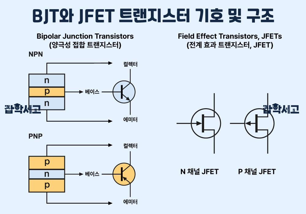
Basic Concepts of the Transistor
The transistor is a key device in modern electronics, mainly performing amplification and switching functions. A transistor has three terminals, through which it can control an input signal to regulate the output signal. Transistors are basic building blocks of various electronic devices and are essential in computers, smartphones, radios, audio equipment, and more. Transistors are divided into two main types: the BJT (bipolar junction transistor) and the FET (field-effect transistor).
BJT: The Current-Controlled Transistor
A BJT (bipolar junction transistor) has three semiconductor regions: the emitter, the base, and the collector. The emitter supplies electrons, the collector collects them, and the base controls the flow of current between them. The key principle of the BJT is that applying a small current to the base allows it to amplify a large current flowing from the emitter to the collector.
BJTs play an important role in amplifiers and are capable of making weak signals much larger. For example, in a radio or audio device, a small input signal passing through a transistor is converted into a larger output signal, amplifying the sound. This amplification function is an important factor that greatly improves the performance of various electronic devices.
FET: The Voltage-Controlled Transistor
A FET (field-effect transistor) consists of three terminals: the gate, the drain, and the source. Unlike a BJT, a FET operates by voltage: when a voltage is applied to the gate, current flows from the source to the drain. Because it is controlled by voltage rather than current, a FET has a higher input impedance than a BJT and can switch faster with less power.
FETs are mainly used as switching devices. A switching device has the ability to quickly block or allow the flow of current, and through this the transistor plays a key role in implementing complex logic circuits in digital circuits such as those in computers and smartphones. Thanks to their high speed and efficiency, FETs are mainly used in electronic devices where high-speed processing and power consumption are important.
The Amplification Function of the Transistor
The amplifying action of a transistor is the function of converting a weak input signal into a strong output signal. This amplification process greatly magnifies small changes in current or voltage, and it plays an essential role in electronic devices such as audio equipment, radios, and TVs. Transistors amplify faint electrical signals, improving signal quality or making it possible to obtain an output signal of the required magnitude.
The amplification function is especially important in analog circuits. In the process of amplifying variations in the input signal and passing them to the output, the transistor makes the original signal larger without distorting it. This plays a key role in providing amplified output while maintaining signal quality in communication equipment and audio devices.
The Switching Function of the Transistor
The switching action of a transistor is a key operating principle in digital circuits. Switching is the function of blocking or allowing current to flow; the transistor blocks or passes current under certain conditions to implement binary states (ON/OFF). Through this, transistors form complex circuits such as logic gates in computers, smartphones, and various other electronic devices.
In digital circuits, transistors can control the flow of current quickly and efficiently, which enables high-speed processing and low power consumption. Through their switching function, transistors play an important role in signal processing and data transmission in a variety of electronic devices.
The Importance of the Transistor
The transistor is an important device that forms the foundation of modern electronics, performing two main functions: amplification and switching. Through amplification it makes weak signals strong, and through switching it plays an important role in processing data in digital circuits. Thanks to these functions of transistors, electronic devices such as computers, smartphones, radios, and TVs can operate properly.
The transistor is a core element of electronic engineering, and a wide variety of electronic devices and systems can be designed based on it. Advances in the transistor have driven the growth of electronics, and it will continue to play an important role in realizing ever more efficient and powerful electronic technologies.
Semiconductor physics is a discipline that provides the fundamental theoretical framework of modern electronics and plays an essential role in the advancement of electronic devices and information and communication technology. Basic concepts such as the movement of electrons and holes, the properties of the conduction band and band gap, and the PN junction are important for understanding the operating principles of devices such as diodes and transistors. These devices are the key components of integrated circuits and form the foundation of the many electronic devices used around the world.
A deep understanding of semiconductor physics is therefore important knowledge that can drive new innovation not only in electronic engineering but also in many other fields such as physics and materials science. Going forward, semiconductor physics will become even more important as a core discipline that enables the advancement of cutting-edge technology and new technological innovation.